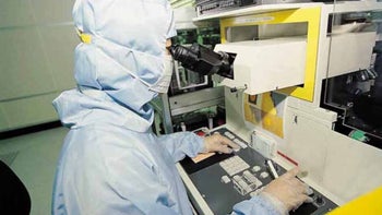
Apple supplier expects to start volume production of 3nm chips as soon as 2022

This year, TSMC debuted chips made using its 5nm process node. The first smartphones released with a 5nm chip were the Apple iPhone 12 series which features the A14 Bionic chipset. Apple also has this chip powering the iPad Air (2020). The 5nm A14 Bionic has a transistor density of 134 million transistors per square mm compared to 89.97 million transistors per square mm on the 7nm A13 Bionic. The transistor count for the A14 Bionic is 11.8 billion compared to 8.5 billion transistors for the A13 Bionic. Those additional transistors found in the A14 Bionic make it a more powerful performer and more energy efficient than the A13 Bionic.
The A16 Bionic could be the first chip built on the 3nm process node
Android phone manufacturers will have their own 5nm chips to use with the Snapdragon 888 or the Exynos 2100. Not only are both produced using the 5nm node, they both are produced by Samsung Foundry. The just announced Samsung Galaxy S21 series uses both chips depending on the region where the device is purchased. Meanwhile, Digitimes reported today that TSMC will start risk production of its 3nm chips this year with volume production beginning during the second half of next year. During the foundry's quarterly earnings report announced on Thursday, TSMC CEO CC Wei said, "Our N3 technology development is on track with good progress. We are seeing a much higher level of customer engagement for both HPC and smartphone application at N3 as compared with N5 and N7 at a similar stage."

pple's A14 Bionic chip was the first 5nm SoC used on a smartphone
If TSMC follows this road map, we should see the iPhone 14 line become the first handsets manufactured by Apple to employ chips produced with the 3nm process node. The first such chip would be the A16 Bionic. This past November, TSMC completed the plant structure for its 3nm fab at the Southern Taiwan Science Park (STSP). TSMC originally planned on starting 3nm trial production at the end of 2020. But the global pandemic forced TSMC to push this back by one year.
Instead of spending $20 billion-$28 billion this year on capital expenditures as estimated by analysts, TSMC says that this range will be higher at $25 billion-$28 billion. The complexity of the technology needed to build 3nm chips is one of the reasons for the higher spending. TSMC is also hemorrhaging cash as it purchases EUV lithography equipment. Extreme Ultraviolet Lithography is used t0 etch extremely thin lines on a wafer. These are the patterns that determine the placements of transistors inside a chip. Considering that billions of transistors are used in each chip, these lines must be as thin as possible and this is where the EUV Litography machine comes into play.
TSMC will use FinFET transistors for its 3nm chips while Samsung will switch from FinFET to GAA (gate-all-around). For 2nm, TSMC will use a GAA design. Samsung reportedly spent approximately for $116 billion to develop its 3nm integrated circuits. We could see mass production of 2nm chips starting in 2024 at the earliest.
The observation made by Intel co-founder Gorgon Moore known as Moore's law called for transistor density to double every other year and over the last few years, we haven't seen the industry adhere to this law perfectly. And now, as 2nm is in range, the question is whether Moore's Law will be able to continue. Foundries have been working on the use of alternative materials that might be able to keep improving chip performance and energy consumption beyond 2nm. Just like EUV helped keep Moore's Law stay valid after the 10nm process node, something new could be found to keep Moore's Law alive.


Things that are NOT allowed: