TSMC tests 2nm production while hiking the cost of silicon wafers by 50% to $30K for this node

The application processor (AP) used to power the first iPhone contained approximately 70 million transistors and was produced using a 65nm process node. While those specs were cutting-edge at the time, 17 years later the A18 Pro AP inside the iPhone 15 Pro and iPhone 15 Pro Max is manufactured using TSMC's second-generation 3nm process (N3E). While Apple has not yet revealed the transistor count for the new chipsets, chances are that the A18 Pro has more than the 19 billion transistors found in the A17 Pro.
Originally it was thought that the iPhone 17 Pro and iPhone 17 Pro Max would be the first smartphones powered by a chip produced using the 2nm node. But TF International Apple analyst Ming-Chi Kuo now says that the 2025 iPhone 17 Pro models will be manufactured using TSMC's third-generation 3nm process node (N3P). The debut of the 2nm chipset on the iPhone will now take place in 2026 with the A20 Pro chipset that will power the iPhone 18 Pro and iPhone 18 Pro Max.
TSMC was charging chip designers $20,000 for each silicon wafer used to produce a 3nm chipset. Each wafer can produce 300 to 400 chips. At $30,000, the wafer used for 2nm production is 50% more expensive than the $20,000 TSMC charged for the wafer used in 3nm production. It is twice as expensive as the $15,000 charged for the wafers used in TSMC's 4nm and 5nm production. Going back even more, in 2014 TSMC charged clients $3,000 for wafers used to build its 28nm chips.
There is a good reason to charge $30,000 for a 2nm wafer. The process node requires more complex and precise manufacturing procedures. In addition, a report from consulting firm IBS says that it costs $28 billion to produce a fab that produces 50,000 wafers a month.
The 2nm node will debut a couple of new features for chips built by TSMC. The foundry's 2nm chips will use nanosheet Gate-all-around (GAA) transistors to replace FinFET. With GAA, the gate comes into contact with the channel on all sides reducing current leakage and improving the drive current. This results in a 10% to 15% power boost, a 15% transistor density increase, and a 25% to 30% reduction in power consumption.
TSMC's 2nm production will also include backside power delivery (BPD) which moves the power connections to the back side of the chip allowing them to be shorter than the connections used with traditional frontside power delivery. This results in a reduction in power loss from line resistance. The bottom line is a 15%-20% improvement in power usage.
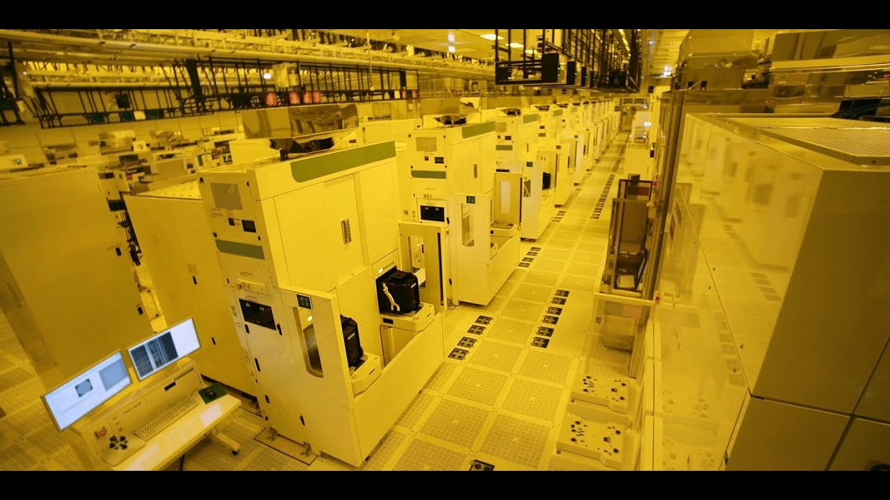
Mass production of TSMC's 2nm chips will start during the second half of 2025. Trial production of 2nm chips has already started at TSMC's Baoshan Plant in Hsinchu, northern Taiwan. Apple supposedly has already reserved all of TSMC's 2nm production for the A20 Pro SoC.
Follow us on Google News


Things that are NOT allowed:
To help keep our community safe and free from spam, we apply temporary limits to newly created accounts: