TSMC's yields on early 3nm production are reportedly as high as 80%

The TSMC-Samsung Foundry rivalry isn't exactly the most famous in the world. It isn't close to being the duopoly that comes to mind first (Coke-Pepsi might be number one) as most consumers couldn't give a damn where the chips inside their phones come from. But the world's largest foundry is TSMC. Apple is the foundry's number one customer accounting for a quarter of its revenue. Samsung and TSMC have at one time or another produced Snapdragon chips for Qualcomm.
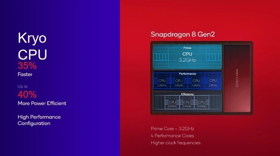
The Snapdragon 8 Gen 2, Qualcomm's new top-of-the-line application processor (AP), is being produced by TSMC with one exception. The overclocked version of the chip being used to power the upcoming Samsung Galaxy S23 series will be made by...Samsung Foundry. The difference is the faster clock speed for the CPU's X-3 high-performance core which will run at 3.32GHz compared to a clock speed of 3.2GHz for the TSMC version.
Samsung Foundry reportedly lost some of Qualcomm's business due to low yields
Samsung was producing last year's Snapdragon 8 Gen 1 chip. But low yields caused Qualcomm to switch to TSMC for the Snapdragon 8+ Gen 1 and the Snapdragon 8 Gen 2. The yield is the percentage of chips produced on a single silicon wafer that passes through quality control. Samsung Foundry has a yield of only 35% for the 4nm Snapdragon 8 Gen 1 chip. Meanwhile, TSMC's yield for its 4nm chips was twice that of Samsung Foundry's at 70%.

TSMC will produce the vast majority of Snapdragon 8 Gen 2 chipsets
This past week, TSMC started mass production of its 3nm chips using its N3 process node months after Samsung Foundry started producing chips using its 3GAE (3nm-class, gate-all-around early) node. As the process node numbers shrink, it is used as a way to mark the beginning of the next generation of cutting-edge chip production. The lower the process node number, the higher the transistor count (the number of transistors inside a chip) making these components more powerful and energy-efficient.
For example, the 2019 iPhone 11 series featured the 7nm A13 Bionic SoC with 8.5 billion transistors inside. This year's A16 Bionic, produced using TSMC's 4nm process node, contains nearly 16 billion transistors.
A report by Tom's Hardware cites analysts contacted by Business Next for estimating that TSMC's N3 yields could be in the 60%-70% range or as high as 75% to 80%. The point is that either range isn't bad at all for the first batch of "cookies" coming out of the oven. One analyst said that TSMC's yield on its early N3 production is similar to the foundry's early N5 (5nm) yield and could be as high as 80%.
Samsung, on the other hand, continues to have issues with yield. Industry sources claim that Samsung Foundry's early-stage yield on its 3GAE production ranged between 10% and 20% which means that it costs more money and takes more time for Sammy to accumulate the same number of chipsets as TSMC. As time goes by, Samsung's yields should improve.
Samsung's 3nm nodes differ from TSMC's in a very important way
We should point out that since most of TSMC's cutting-edge production is created for Apple, it would be easier for it to achieve a higher yield than Samsung this early in the 3nm era. Apple might be the only TSMC customer to order N3 production while other customers wait for the next stage of this node which would be N3E. As a result, it might not be completely fair to compare yields between the two rivals although there does appear to be a huge gap between them.
Samsung's 3nm chips have a major structural difference from TSMC's. Samsung is using gate-all-around (GAA) transistors which allow for more control over the current flow of a transistor. This is because GAA transistors have vertically stacked nanosheets to cover all four sides of the channel for more control and less leakage. TSMC's 3nm node still uses FinFET transistors that have horizontally placed "fins" that cover only three sides of the channel. TSMC will switch to GAA for its 2nm production.
2nm production is indeed lurking around the corner with both TSMC and Samsung looking to start churning out such chips in 2025. Samsung's road map calls for a 1.4nm node in 2027 while TSMC has talked vaguely about 1nm.


Things that are NOT allowed: