The transistor density of TSMC's 3nm chips will blow your mind

Taiwan Semiconductor Manufacturing Company (TSMC), the world's largest independent foundry, takes chip designs made by companies like Apple, Qualcomm, and Huawei and manufactures the final product. One equation remains the same no matter which customer TSMC is assembling chips for; the more transistors inside a chip, the more powerful and energy-efficient it is.
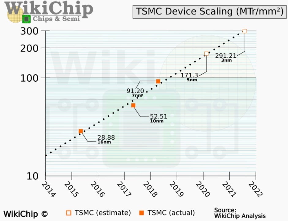
The process node used by a foundry relates to the number of transistors that fit inside a specified space, such as a square mm. For example, the transistor density of the chips currently produced using the 7nm process (such as Apple's A13 Bionic, Qualcomm's Snapdragon 865 Mobile Platform, and Huawei's Kirin 990 5G chipset) is approximately 100 million transistors per square mm. That allows Apple to stuff 8.5 billion transistors into each A13 Bionic SoC. The new 5nm chips rolling off the assembly line this year will have 171.3 million transistors per square mm which will allow the 5nm A14 Bionic to contain 15 billion transistors inside. Performance of the new chips will increase 10-15% while energy consumption will decline by 25%-30%.
TSMC's 3nm chips will have a transistor density of nearly 300 million transistors per square mm
Moore's Law, an observation made by Intel co-founder Gordon Moore back in the 1960s, originally called for transistor density to double every year. In the 1970s, he revised that to every other day. Many have called for the "law" to be repealed especially with density rates so amazingly high. Moore's Law hasn't been adhered to perfectly, but the general concept of the observation still holds.

The transistor density of chips keeps going up as the process node goes down
Right now, TSMC and Samsung are racing to complete facilities to produce 3nm chips. Recently, both foundries noted that the coronavirus outbreak is pushing back their timelines for this process node. According to WikiChip, TSMC's 3nm chips will deliver a 5% performance boost while consuming 15% less energy. And the transistor density will rise by 1.7 to just shy of 300 million transistors per square mm. Amazing. TSMC is expected to begin risk production of 3nm chips in 2021. Those are orders from customers willing to purchase the chips without having them fully tested. Volume production will begin in the second half of 2022 with mass production possibly starting the following year. A recent report stated that due to the current crisis, Samsung is pushing back its 3nm Volume Production from 2021 to 2022.
TSMC and Samsung are taking different approaches to 3nm. The former is using the FinFET transistors for 3nm. The FinFET design helps control the flow of current and voltage in a circuit. Samsung is prepared to leave FinFET for MBCFET (Multi-Bridge-Channel FET, multi-bridge-channel field effect tube) technology. Compared to the current 7nm chips employed at this very moment, Samsung's 3nm chip will provide a 35% performance boost with 50% less energy consumption. MBCFET uses a new technology called Gate All Around (GAA) which makes transistors smaller and more powerful. According to one consultant, "Samsung is ahead of TSMC in GAA by probably 12 months. Intel is probably two to three years behind Samsung." Ryan Lee, Vice President, Foundry Marketing at Samsung said, "Gate all around will mark a new era of our foundry business."
But before we can dream of 3nm, there is the launch of devices running on 5nm chips that will take place later this year. If all goes as planned, the 2020 5G Apple iPhone 12 family will be the first smartphones to use a 5nm chipset. These devices should be unveiled in September and released in October or November. The first Android phones to sport a 5nm chip will be the Huawei Mate 40 series (although it won't feature Google Mobile Services).


Things that are NOT allowed: