TSMC's test run of 2nm chips results in a yield just short of what's acceptable for mass production

When it comes to the word "yield," there are many different meanings. For a chip foundry, yield means the percentage of usable chips diced from a silicon wafer that passes quality control. If a foundry has a low yield, it makes the chip cost more expensive since a larger number of wafers are required to manufacture the number of chips needed. That results in lower profit margins, and possible supply shortages.
With the world's leading contract foundry, TSMC, starting mass production of 2nm chips next year, a trial run of the process node by the foundry resulted in yields of 60% or more. The trial run is taking place at TSMC's fab in Zhuke Baoshan located in Taiwan's Hsinchu county. Apple will reportedly stick with TSMC's 3nm node for next year's A19/A19 Pro application processors to be used to power the iPhone 17 line. Those SoCs will be produced using the foundry's third-generation 3nm node (N3P).
Typically a yield of 70% or higher is required for a foundry to mass produce a chip at a given process node. With a 60% yield reported on these 2nm test runs, TSMC should be able to get the yield into the acceptable range by next year. According to one report, the first Apple product to feature a 2nm application processor could be the next-gen iPad Pro in late 2025. The first iPhone handsets that will feature a 2nm AP will be 2026's iPhone 19 line.
To understand why the process node is so important just keep one simple thing in mind: as process numbers go lower, transistor sizes typically get smaller. This increases the transistor count and the transistor density of the chip. The former is the raw number of transistors shoehorned into a chip while the latter is the number of transistors squeezed into a specific area of the chip. Higher numbers for both usually result in a component that is more powerful and/or energy efficient. So as process number shrink, performance and efficiency increase.
TSMC's 2nm node includes a new transistor called Gate-All-Around (GAA). Using vertically positioned horizontal nanosheets, GAA transistors surround the channel on all four sides. The previous generation of transistors, known as FinFET, only covered the channel on three sides. GAA transistors have less leakage and higher drive currents resulting in improved performance.

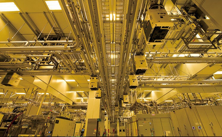
Inside of a TSMC fab in Taiwan. | Image credit-TSMC
While TSMC's 2nm testing has resulted in a 60% yield that could hit the 70% and higher range when 2nm production starts next year, its main rival, Samsung Foundry, continues to struggle with low yields. Last month Samsung denied a rumor that it was canceling the Exynos 2600 which is expected to be built by Samsung Foundry using its 2nm node. The rumor called for Samsung to cancel the chip because of Samsung Foundry's low 2nm yields rumored to be in the range of 10% to 20%.
This wouldn't be the first time that Samsung Foundry has been penalized for having low yields. Back in 2022, Samsung Foundry's low yields on production of the Snapdragon 8 Gen 1 led Qualcomm to yank its business away from Samsung Foundry and turn it over to TSMC. That resulted in the development of the Snapdragon 8+ Gen 1. Since then, Qualcomm's flagship smartphone application processors have been built by the Taiwan-based foundry.


Things that are NOT allowed: