SMIC's N+1 process node not enough to save Huawei

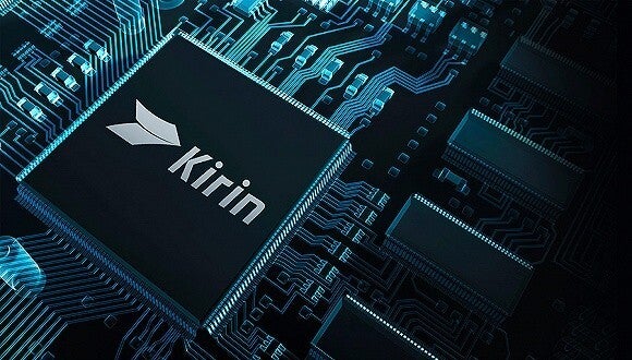
2020 was going to be a big year for Huawei. As TSMC's second-largest customer after Apple, the Chinese manufacturer was set to receive its first 5nm chipset, the Kirin 9000. Apple's A14 Bionic and Huawei's Kirin 9000 were the first integrated circuits to be produced using a 5nm process node allowing more transistors to be employed. For example, the 5nm Kirin 9000 is packed with approximately 171.3 million transistors per square mm. That compares to the roughly 100 million transistors per square mm found on the 7nm Kirin 990 5G chipset. The higher the number of transistors packed in a dense spot, the more powerful and energy-efficient a chip is.
SMIC closing in on 7nm process node but it might be too little too late for Huawei

The Kirin 9000 is made using TSMC's 5nm process node
Huawei had been in discussions with Semiconductor Manufacturing International Corporation (SMIC), the largest foundry in China. But there was a bit of a problem. SMIC's most advanced process node is 14nm. While the transistor density for TSMC's 5nm chip is approximately 171.3 million transistors per square mm, the 14nm process node carries roughly 43 million transistors per square mm. While SMIC did make a mid-range 14nm Kirin 710A chip for Huawei, the latter really needs to find a replacement for TSMC that can deliver 5nm chips without violating U.S. export rules. In other words, a 14nm chipset is not powerful enough to drive the Mate 40 line, the Mate X2, and 5G base stations.
SMIC is working on its N+1 node that is being called 8nm or an early stage of its 7nm process by the Chinese media. According to China's Zhuhai Special Zone Newspaper, SMIC has completed the first tape out and testing of this node. This is the final stage in the chip manufacturing process and is done to make sure that there are no issues or kinks that need to be worked out before the chip starts rolling off of the assembly line.
The N+1 node improves performance by 20% while reducing power consumption by 57%, logic area by 63%, and system-on-chip (SoC) footprint by 55%. Compare that to TSMC's 7nm process which improved transistor density by approximately 73% over its 10nm node and delivered 35-40% speed improvement with 65% lower power draw its 16nm node. As a result of the low 20% performance improvement, SMIC won't call N+1 a pure 7nm node despite the similarities in some of the other numbers. There should be three generations of this node including N+1 node, N+2, and N+3. SMIC is hoping to receive advanced lithography equipment before N+2 is produced. The equipment, from industry leader ASML, allows very thin lines to be marked up on a die so that a large number of transistors can be deployed.
Eventually, SMIC could be ready to manufacture 5nm chips for Huawei but by the time this happens, TSMC will be on the 3nm node. For Huawei to stay competitive with Apple and Samsung, it won't be able to count on SMIC right now. Without access to a top foundry and cutting-edge chips, Huawei would still be able to manufacture mid-range models but would not be able to churn out its top-selling flagship phones.


Things that are NOT allowed: