Samsung rumored to begin mass production of 3nm chips next week

Right now there are only two independent foundries that are able to manufacture cutting-edge chips. The companies are TSMC and Samsung Foundry. Independent foundries take chip designs created by other firms and build the actual chips off of that design. Both TSMC and Samsung are working on building chips using their 3nm process nodes. The smaller the process node used, the larger the number of transistors found inside a chip.
Samsung is rumored to announce mass production of 3nm chips as soon as next week
This is important because the more transistors employed in a chip, the more powerful and energy-efficient that chip can be. Every two years or so, the process node gets smaller and more transistors fit inside an integrated circuit. This is the famous "Moore's Law" that you've heard about, named after Intel and Fairchild semiconductor co-founder Gordon Moore. Remember, this is not an actual law and as smaller and smaller components are being built, this "observation" no longer can be fully counted on to double the transistor count every other year.


Still, over time, you can see how "Moore's Law" has forecast the incredible increase in processing capabilities over the years. Let's take the iPhone X, which was released in November 2017 powered by the Apple A10 Bionic chipset. The latter carried 4.3 billion transistors in each chip. Now let's move ahead to the 2021 iPhone 13 series which sports the A15 Bionic chipset. The A15 Bionic contains 15 billion transistors, up 27.1% from the 11.8 billion transistors employed by the A14 Bionic chip.
So now Samsung and TSMC are battling for supremacy in the business of building chips for third-parties. TSMC is number one in most metrics and its customer list includes top tech firms such as Apple (its number one customer), MediaTek, Nvidia, Qualcomm, and others. But it appears, according to ExtremeTech, that Samsung will soon beat out TSMC by starting mass production of chips made using its 3nm process node next week with TSMC starting 3nm mass production later this year.
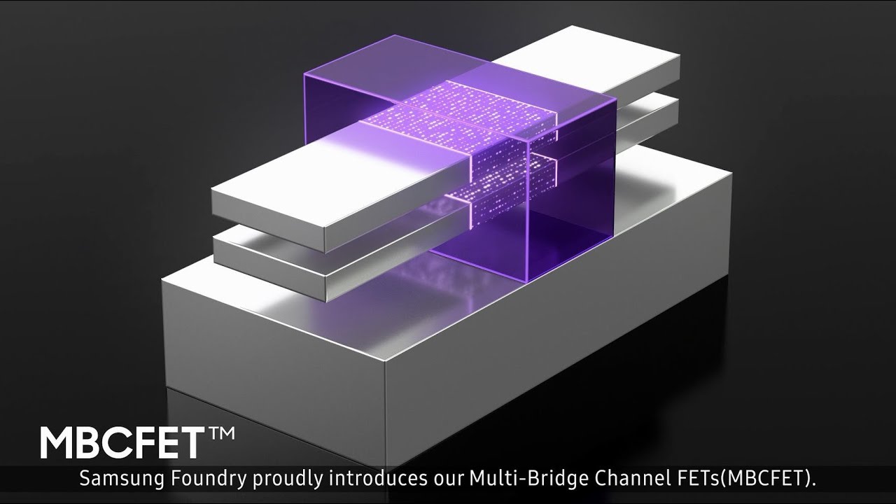
Additionally, Samsung is going to use a new transistor structure on its 3nm chips called GAA or gate-all-around. With this structure, the flow of current is controlled by gates that contact the transistor on all four sides. TSMC will continue to use the FinFET structure which has been in place since the 22nm process node debuted. TSMC will finally scrap FinFET for GAA when it starts shipping 2nm chips in 2026.
Samsung's GAA design is called Multi-Bridge Channel Field Effect Transistor (MBCFET) also known as nanowires. This is one of only two different gate-all-around designs currently available with the second one known as GAAFET or nanowire.

Transistor architecture moves from FinFET to gate-all-around
The report cites a major Korean news agency that says Samsung is expected to make a major announcement about its 3nm chip production shortly. It also notes that the move to gate-all-around from FinFet will reduce the area of a chip by 45% to help deliver a performance bump of 30% while reducing energy consumption by 50%. However, there is a big problem. Samsung was reportedly getting yields of only 10% to 20% at 3nm meaning that the vast majority of its 3nm chip dies cut from a wafer could not pass quality control.
Back in February, a report indicated that Samsung's yield on 4nm production was only 35% resulting in Samsung losing some business from chip designer Qualcomm. The latter supposedly moved some of those orders to TSMC. However, if Samsung Foundry is about to announce the start of high volume manufacturing (HVM) at the 3nm process node, one could come to the conclusion that Samsung Foundry has improved its 3nm yield.
Speaking of 3nm, Digitimes reported that TSMC's major customers such as AMD, Apple, Broadcom, Intel, MediaTek, Nvidia, and Qualcomm, have started to queue up for 3nm capacity. And next on the horizon, of course, is the 2nm process node that both TSMC and Samsung are working on. Another name is expected to join TSMC and Samsung on the list of cutting-edge foundries. Intel Chief Executive Pat Gelsinger has announced that the American company will regain process leadership from Samsung and TSMC by 2025.


Things that are NOT allowed: