With a low 20% yield for second-gen 3nm chip production, Samsung Foundry looks ahead to 2nm

Samsung Foundry could have had a big advantage over TSMC at the 3nm process node. That's because, unlike TSMC, Samsung Foundry decided to use Gate-All-Around (GAA) transistors for its 3nm production. These transistors use vertically placed horizontal nanosheets to surround the channel on all four sides reducing current leaks and improving the drive current. As a result, SoCs made with GAA transistors typically offer improved performance with reduced power consumption.
This should have given Samsung Foundry an edge at the currently used second-generation 3nm node since leading foundry TSMC still uses FinFET transistors which surround the channel on only three sides. TSMC will switch to GAA next year when it starts mass production of its 2nm chips. But there is one main reason why TSMC continues to take business from Samsung Foundry and that is related to the latter's extremely poor yield.

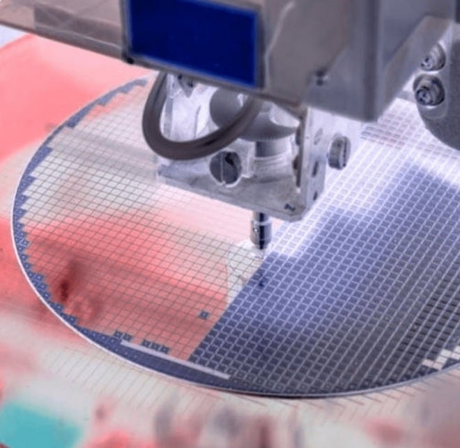
Samsung Foundry is having yield problems with its 3nm process node. | Image credit-Samsung Foundry
The yield is the percentage of good chips that pass quality control divided by the maximum number of chips that could be produced from a single silicon wafer. For its 3nm GAA production Samsung reportedly expected yields to hit 70% and for the first generation of the 3nm node (aka SF3E-3GAE) the yield was between 50% and 60% which was just shy for the 70% that might get fabless chip designers to choose Samsung Foundry to build their components.
For the second-generation 3nm node, yields are even worse for Samsung Foundry. At 20% for this production, chip designers will run from Samsung Foundry since the designers are the ones taking the financial hit for the lost production. The low yields explain why TSMC is building the Snapdragon 8 Elite application processor that will power the Galaxy S25 Ultra next year. Even South Korean chip designers who previously ordered from Samsung Foundry have decided to go with TSMC instead.
The yields for Samsung Foundry's first and second generation 3nm node were posted by yeux1122 in a blog published by South Korean search firm Naver.
With its 3nm yields terribly low, Samsung is supposedly moving ahead and is working on its 2nm node. A previous rumor called for Samsung Foundry to develop and manufacture an unnamed Exynos chipset on the SF2P 2nm node. The chip is codenamed 'Ulysses,' and it could debut on one of the Galaxy S27 models released in 2027.


Things that are NOT allowed: