Report explains why Samsung Foundry's 2nm chips next year will be more powerful and energy-efficient
Samsung Foundry is expected to start producing chips using its first-generation 2nm process node next year. By reducing the size of the chip's feature set roughly every other year, the size of the transistors get smaller allowing transistor density to increase. Higher transistor density typically indicates a more powerful chip with improved energy efficiency. The Elec says that it has discovered that Samsung Foundry's 2nm node will increase the number of EUV layers by 30%.
EUV is the extreme ultraviolet lithography machine made by one company in the whole world, Dutch firm ASML. The device etches circuitry patterns onto silicon wafers using extremely thin lines to help with the placement of components placed inside a chip. Multiple layers are required for the processors used in smartphones.
Samsung Foundry will use approximately 26 EUV layers for its 2nm production next year
Samsung Foundry currently uses 20 EUV layers with its current 3nm production and a 30% increase would result in 26 layers for its 2nm chips. More EUV layers should result in more transistors found inside a chip making the SoC able to handle more complex tasks while consuming less battery power. Samsung's 2nm chipsetsd will be 17% smaller than the current-generation chipsets, 18% more powerful, and 15% more efficient.
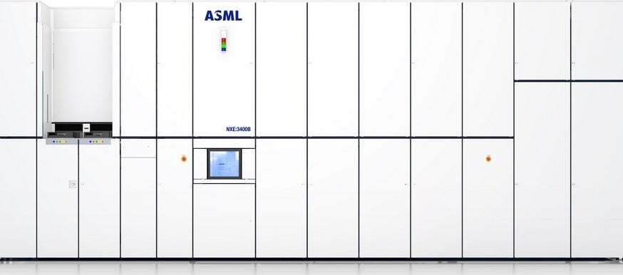
ASML expects to ship 60 of these first-generation EUV lithography machines this year. | Image credit-ASML
Besides using an increased number of EUV layers, at 2nm Samsung Foundry will use backside power delivery network (BSPDN). This tech is responsible for the 17% decline in chipset size by moving the power supply lines to the backside of a chip instead of the front. This reduces voltage drop because the lines can be made bigger thanks to having more room. This technology, also used by Intel with its PowerVia feature, makes chipsets more powerful and efficient.
Looking ahead to 2027 when Samsung Foundry is expected to begin production using its 1.4nm node, the number of EUV layers is expected to rise to more than 30. And once again the transistor count will rise and application processors will be more powerful and energy-efficient than they are today. Samsung Foundry's chief rival is industry leader TSMC and the Taiwan-based foundry uses up to 25 EUV layers for its current 3nm (N3x) production.
Samsung Foundry started employing EUV lithography in 2018 when it moved from 10nm to 7nm. Before EUV lithography, the industry used DUV (or deep ultraviolet) lithography. Samsung Foundry is also using EUV for DRAM production with seven layers used in the manufacturing of its Gen 6 10nm DRAM chip. SK Hynix, another DRAM designer and manufacturer, uses five EUV layers.
Only one company makes and sells EUV machines
ASML is expecting to ship even more EUV lithography machines this year. Each one is the size of a school bus and costs up to $183 million for the previous-generation model and up to $380 million for the High-NA second-gen machine. TSMC will reportedly receive 70 first-generation EUV machines from ASML in 2024 and 2025 due to the strong demand for chips produced using its 3nm and 2nm nodes. Like Samsung Foundry, TSMC will start producing 2nm chips next year with its 1.4nm node expected to be employed in 2027-2028.
The EUV lithography machine has been the driving force allowing foundries to take their process nodes from double-digits to the current 3nm. Now the new generation High-NA machine has been released by ASML, and to keep the new machines out of TSMC and Samsung Foundry's hands, Intel has purchased every single unit shipped to date.
While the previous-generation EUV machines have an aperture of .33, the High NA machines have an aperture of .55. Using the High-NA machine, a higher resolution pattern is transferred to a wafer so that a foundry doesn't have to run a wafer through the EUV machine twice to add additional features. This saves both time and money. Samsung Foundry has reportedly purchased at least one High-NA lithography machine but TSMC refuses to purchase one of the new generation EUV machines for now.
Follow us on Google News


Things that are NOT allowed:
To help keep our community safe and free from spam, we apply temporary limits to newly created accounts: