Despite being handicapped by U.S. sanctions, Huawei and SMIC have a plan to produce 3nm chips

It's quite possible that the U.S. sanctions that were intended to prevent Huawei from obtaining cutting-edge chips could fail. That's because Huawei filed a patent to use self-aligned quadruple patterning (SAQP) lithography to build 3nm chips using multi-patterning techniques. The multi-patterning techniques are the subject of another patent filed by state-funded chip manufacturing company SiCarrier which, according to Tom's Hardware, confirms that China's largest foundry SMIC is interested in using SAQP to produce 3nm chips for Huawei using Deep Ultraviolet (DUV) lithography machines.
Currently, only TSMC and Samsung Foundry are building 3nm smartphone chipsets which currently require the use of Extreme Ultraviolet lithography (EUV) to etch the extremely thin, high-resolution circuitry patterns on silicon wafers. While U.S. sanctions prevent "cutting-edge" chips from being supplied to Huawei by foundries using U.S. technology, there is only one company, ASML, that makes EUV machines and the Dutch have banned the firm from shipping the school-bus-sized machines to Chinese companies.
Hundreds of chips are built on each wafer and the circuitry patterns etched on each wafer must be thin enough to accommodate the billions of transistors found inside the chips. As the process node number drops, so does the size of the transistors used which allows more to be stuffed inside each chip. Typically, the higher a chip's transistor count, the more powerful and/or energy-efficient that chip is. For example, the 7nm A13 Bionic SoC that powers the iPhone 11 series carries 8.5 billion transistors. The 3nm A17 Pro SoC used on the iPhone 15 Pro and iPhone 15 Pro Max is equipped with 19 billion transistors.

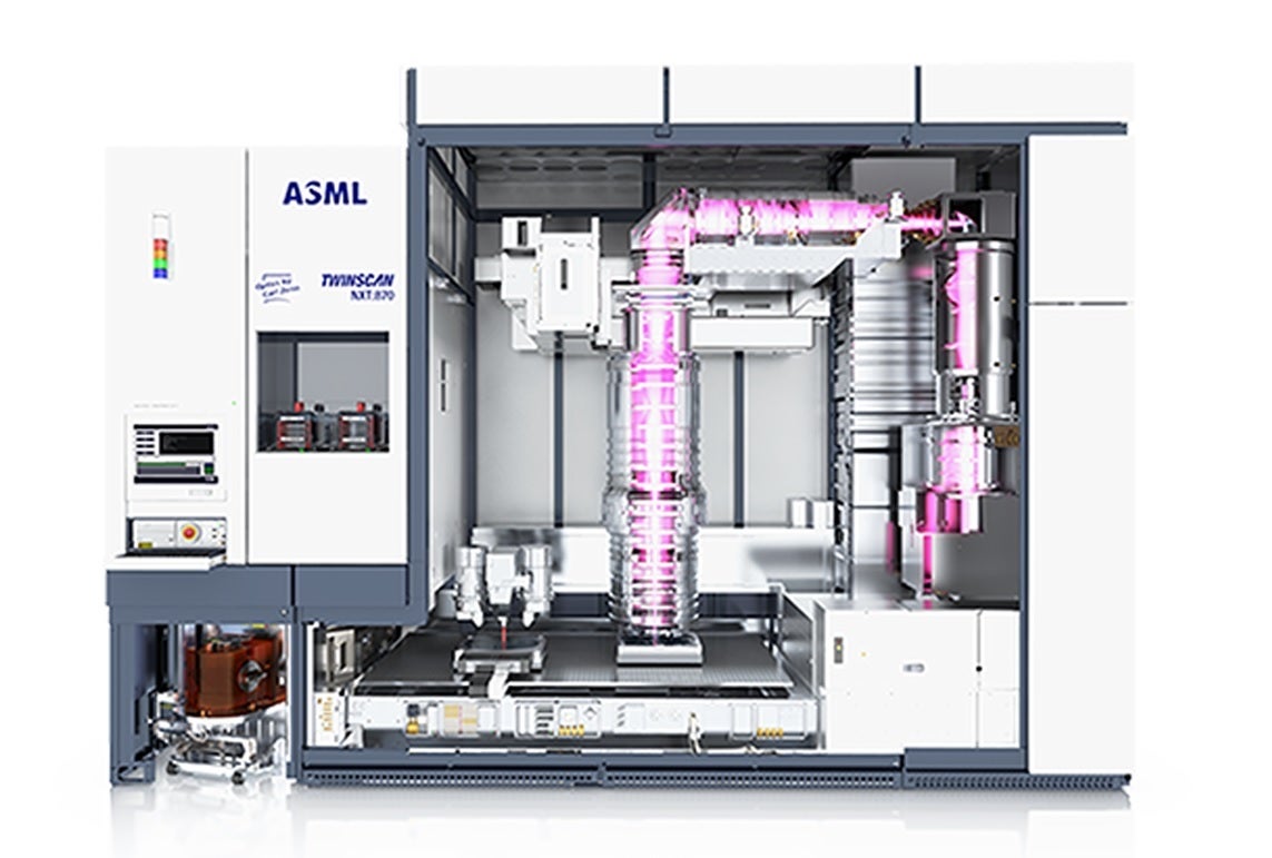
Huawei hopes that the use of SAQP, multi-patterning, and a DUV lithography machine (pictured) will allow it to obtain 3nm chips
Experts agree that Huawei and its chip manufacturer SMIC might be able to use SAQP, the previous generation's Deep Ultraviolet Lithography machines, and multiple patterning to produce 5nm chips. However, these experts state that EUV is needed for 3nm silicon. Even then, double-patterning is needed to produce 3nm chips using Low-NA EUV tools. Without making this more complicated than it is already, let's just say that Huawei and SMIC believe that with SAQP, they will be able to make 3nm chips using older and less capable DUV machines that were purchased by SMIC before the sanctions took effect.
If you think that U.S. lawmakers and officials were pissed when Huawei announced that the Mate 60 series last August was powered by the 7nm Kirin 9000s 5G chip, imagine the response if Huawei is able to obtain 3nm chips from SMIC. The sanctions originally forced Huawei to use Snapdragon chips obtained from Qualcomm on the 2022 flagship P50 and Mate 50 models, and 2023's Mate 50 line. Qualcomm obtained a license from the U.S. Commerce Department allowing it to ship the chipsets to Huawei which were tweaked to prevent them from working with 5G signals. Those licenses have been lifted by the U.S. Commerce Department.
While the 7nm Kirin 9000s application processor (AP) is two generations behind the 3nm A17 Pro AP that powers the iPhone 15 Pro series, the chip does support 5G which made the Mate 60 line the first Huawei flagship series since 2020's Mate 40 line to offer Chinese consumers 5G connectivity.


Things that are NOT allowed: