This one $300 million machine will help build powerful chips under 3nm
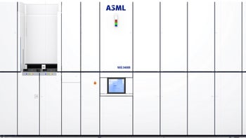
You might not have ever thought about it, but the smaller the size of the transistors used in chips, the thinner the markings need to be on wafers that show where a chip's circuitry will be placed. Photo masking used to be the way that circuit patterns were transferred to wafers, but this process was about to be obsolete when Dutch manufacturer ASML created extreme ultraviolet lithography (EUV), a machine that allows extremely thinner patterns to be "printed" on wafers.
ASML's High NA second-generation EUV will allow foundries to produce chips using a process node under 3nm
EUV is credited with extending Moore's Law below 10nm and back in September we told you about the company's second-generation EUV machine; the next version of ASML's ultraviolet lithography machine is back in the news thanks to a CNBC report. Intel, by the way, announced this past summer that it will be the first recipient of the next-gen ASML machine. It was the chipmaker's CEO Pat Gelsinger who made that comment and also revealed that the new machine is named High NA.
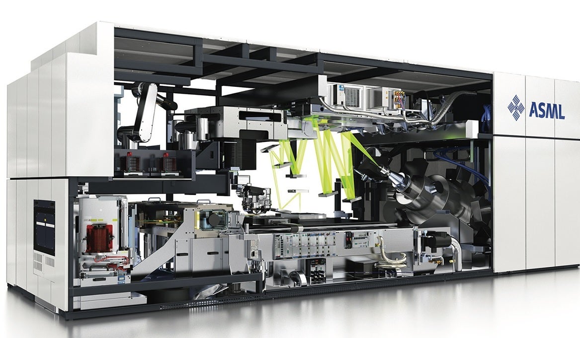
A current generation EUV machine made by ASML and priced at approximately $140 million
High NA actual stands for high numerical aperture. The current EUV machines have an NA of .33, but ASML and ZEISS have been testing machines with an NA of .55.
The higher the NA number, the higher the resolution of the pattern being transferred to a wafer. This could stop foundries from having to run a wafer through the EUV machine a second time to add additional features to a pattern.
The original EUV machines are used by companies that you would expect to own one such as TSMC and Samsung, the world's two largest independent foundries and the only companies that are currently manufacturing 5nm chipsets.
These machines focus narrow beams of light on the aforementioned wafers once they have been treated with "photoresist," a material that is sensitive to light. An ASML spokesman told CNBC about High NA, "It includes a novel optics design and requires significantly faster stages." The higher resolution will enable 1.7x smaller chip features and 2.9x increased chip density.
The spokesperson also mentioned some of the things that we have already covered, but let's hear it again directly from an ASML representative. "With this platform, customers will reduce the numbers of process steps,” the spokesperson added. "This will be a strong motivation for them to adopt the technology. The platform will offer significant defect, cost and cycle time reductions."
The new EUV machines will carry a price tag close to $300 million
And what wasn't mentioned is that the new machine could reduce the time it takes to bring a chip to market, not a little feature in such a dog-eat-dog industry. But the most important feature is the one mentioned by Chris Miller, an assistant professor at the Fletcher School of Law and Diplomacy at Tufts University. Miller says that the goal with the next-generation EUV machine is to use the narrowest wavelength of light possible in lithography so that the foundries can fit more transistors onto each wafer.
About ASML Miller says, "They’re not resting on their laurels." He points out that the High NA machine will allow chip designers to create custom patterns on their components.
In 2024 and 2025, customers will be able to use High NA for their own research and development. Starting in 2025, you can expect foundries to use High NA for their high-volume chip manufacturing.
Gartner semiconductor analyst Alan Priestley says that the new EUV machine will allow chip manufacturers to build chips using a process node under 3nm. Right now we are at 5nm with 3nm chips expected to be ready for volume production at the end of next year.
Each EUV is an expensive investment for a foundry with a price tag in the neighborhood of $140 million each for the currently available machines. Currently used EUV machines contain over 100,000 parts and it takes 40 freight containers or four jumbo jets to ship each one. The first High NA machines will be ready in 2023 as ASML continues working on them, and will carry a price tag close to $300 million.







Things that are NOT allowed: