Apple has sharply reduced the size of the order it has with TSMC

Taiwan Semiconductor Manufacturing Co. Ltd., better known as TSMC, is the world's largest foundry. Only TSMC and Samsung currently mass-produce chips using their respective 3nm process nodes (which use different types of transistors as we will explain later). Apple is TSMC's largest customer and is believed to account for a quarter of the company's revenue (that's 25% for you numerical types).
With the overall weakness of the global economy and the hangover from last year's chip shortage, some major brands have been canceling orders placed earlier with TSMC. And believe it or not, that goes for Apple as well. You know that we often cite Twitter tipsters and for the sake of alliteration, we also check out social media posts from Weibo writers. Weibo is a Chinese social media site and one subscriber, whose user name translates to something like @CellPhoneChipExpert (via GizChina) posted some big Apple news.
Apple reportedly has reduced its TSMC orders by as many as 120,000 wafers
The tipster, who allegedly gets news directly from the semiconductor industry, says that Apple has reduced its orders with TSMC by as many as 120,000 wafers. The canceled orders were for chips that would be made using TSMC's N7, N5, N4, and even some N3 nodes. Rumors call for the A17 Bionic, which is expected to be found under the hoods of the iPhone 15 Pro and iPhone 15 Ultra, to be produced using TSMC's N3 (3nm) process node. Apple's M2 Ultra and M3 chips might also use the same node.

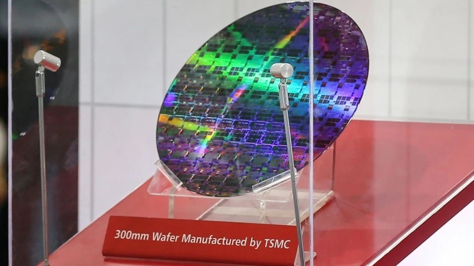
A silicon wafer which is used to produce chips
Digitimes reports that TSMC has been able to beat out Samsung Foundry when it comes to signing up customers. Samsung's 3nm node uses Gate-All-Around (GAA) transistors that allow the gate to come into contact with the channel on all sides resulting in less current leakage and higher drive current compared to the FinFET transistors used by TSMC for its 3nm node. GAA features vertically placed horizontal nanosheets while FinFET uses horizontally placed vertical "fins." TSMC is expected to go to GAA for its 2nm production in 2025-2026.
Despite sticking with FinFET for 3nm production, TSMC still has a pretty full-order book with big names like Qualcomm, MediaTek, and Nvidia reserving production capacity for 2023 and 2024. Samsung, though, has been handicapped in its efforts to secure more business due to low yields. That means that a higher percentage of the chips it cuts from wafers fail to pass quality control.
Wafer prices have risen sharply over the years
The report says that in order to give Apple most of the 3nm production capacity later this year, Intel agreed to change its roadmap and delay receipt of its 3nm orders. TSMC's enhanced 3nm process node (N3E) could be launched this year even though there might not be a big rush for orders considering the cost.
Digitimes points out that wafer prices have skyrocketed with 90nm wafers selling for about $2,000 in 2004. By 2016, 10nm wafers cost $6,000 and that price hit $16,000 for 5nm which debuted on consumer electronics in 2020. Wafer prices for 3nm chips are priced in the $20,000 area.
Intel has said that it will take process leadership from TSMC and Samsung by 2025 thanks to two developments. It will use RibbonFET transistors which is another term for the Gate-All-Around (GAA) transistors already employed by Samsung. And it will use a feature known as PowerVia or backside power delivery. This allows transistors to obtain power from one side of a chip while using the other side to connect to data communication links.
Today's chip designs have transistors trying to handle both functions from the same side which makes the process more complicated and limits the use of miniaturization. Intel will also be the first to use high numeric aperture Extreme Ultraviolet Lithography (EUV). This machine will etch higher-resolution circuitry patterns on wafers which could reduce the time it takes to add additional features to a pattern.


Things that are NOT allowed: