Seeking to regain process leadership from TSMC, Intel refused to make the same mistake twice

Close to a year ago, Intel released a video showing the company receiving its $400 million High-NA EUV, the second-generation of ASML's extreme ultraviolet lithography machines. The original EUV was the indispensable tool that chip foundries needed to take their process nodes under 7nm. Lithography machines help transfer circuitry patterns onto the silicon wafers that are the foundation of chip production.
The new High-NA EUV machines are made only by Dutch firm ASML and Intel was the first foundry to take delivery of the new machines. They offer an increase in numeric aperture (which is what the NA stands for in the machine's name) to .55 from .33 allowing for sharper images and smaller features to be printed on the silicon wafers. This allows foundries to build chips using process nodes under 3nm.
The High-NA EUV lithography machines require less time and money to transfer circuitry patterns to silicon wafers
Lower process nodes typically use smaller transistors which means that more of these important "building blocks" can be shoehorned inside a particular area of an integrated circuit. A higher transistor density makes a chip more powerful and/or energy efficient. The new High-NA machines need fewer exposures to print the designs on silicon wafers allowing Intel to save time and money. What took earlier EUV machines three exposures and approximately 40 processing steps can be done with the High-NA EUV machines with just one exposure and a single digit number of processing steps.
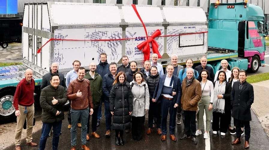
ASML employees stand in front of a box containing an unassembled High-NA EUV lithography machine before it was shipped to Intel. | Image credit-ASML
Yesterday, Intel said at a conference in San Jose, California that the first two High-NA machines it purchased are in production meaning that they are being used in the process of manufacturing chips. Intel says that the new machines are about twice as reliable as the original EUV machines. According to Intel senior principal engineer Steve Carson, his company has produced 30,000 wafers (each wafer can contain thousands of chips depending on yield) using the school bus sized High-NA lithography machines. Carson says, "We're getting wafers out at a consistent rate, and that's a huge boon to the platform."
Intel Foundry Services (IFS) seeks to recapture process leadership from TSMC and Samsung Foundry. Intel's A18 node, set to start mass production in the second half of this year, is similar to TSMC and Samsung Foundry's 2nm node both of which will also start mass production in the second half of 2025. Intel does have a brief window of opportunity since it will be the only foundry using the Backside Power Delivery (BSPD) feature it calls Power Via for several months.
After waiting seven years to use the OG EUV machines, Intel lost process leadership to TSMC and Samsung Foundry
This feature moves the power wiring to the backside of chips leading to more efficient delivery of power to the chip's transistors allowing them to run at higher speeds. TSMC plans to include Backside Power Delivery with the use of its second-gen 2nm node (N2P) set for mass production next year.
Intel lost process leadership when it took the company seven years before it felt that it could rely on EUV lithography allowing TSMC and Samsung to surpass it. Additionally, Intel had issues building chips at 10nm partially due to its reliance on older lithography equipment. Its decision to jump out quickly to buy High-NA EUV machines indicates that it didn't want to make the same mistake twice.
The High-NA EUV lithography machine will be used to help produce chips using Intel's 18A process node. This will be used on a chip codenamed Panther Lake that will be earmarked for use on notebook computers. The new lithography machines are expected to get a heavy workout when Intel starts using them for its 14A node. There is no scheduled production date yet for that node.


Things that are NOT allowed: