Samsung Galaxy S5 teardown reveals all its innards
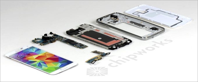
- QFE1100 (Envelope Tracking Power Amplifier PMIC),
- WFR1620 (RF Receiver),
- WTR1625L (RF Transceiver),
- MSM8974AC (Snapdragon 801 (BB/AP SoC)),
- WCD9320 (Audio Codec) and
- PMC8974 (BB/AP Power Management).
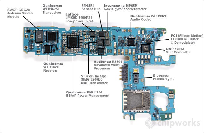
Breakdown of the chips in the Galaxy S5
Probably the biggest change in the Galaxy S5, however, comes in its image sensor. The Galaxy S4 (with the IMX135 Exmor-RS stacked chip), S III and the Note III all used Sony sensors for their camera, while the S5 is the first major Samsung launch in recent history shipping with its own, in-house ISOCELL technology. ISOCELL comes with the ambition to be the next big thing in mobile photography after backside-illuminated sensors (BSI), and it’s got the numbers to prove this: the ISOCELL tech secures 30% reduction in crosstalk and 30% growth in full well capacity. What’s particularly interesting is that now we also see a cross-section portrayal of Samsung’s earlier 8-megapixel ISOCELL tech, and while it’s not the same chip used in the S5, the underlying technology should be very similar, if not identical.
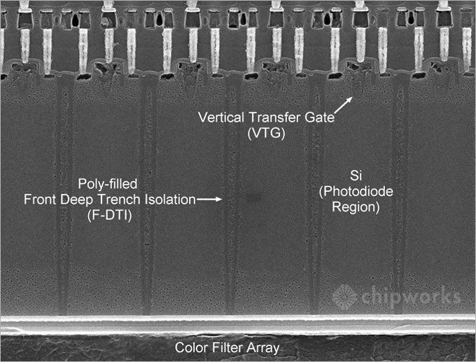
Samsung is not sitting still with ISOCELL either, so we can only expect the technology to improve in the near future. Just over a month ago, Samsung unveiled a new stacked 13-megapixel ISOCELL chip that is scheduled for mass production in the second quarter of 2014. Plenty to look forward to, but right now you can hit the source link below for the full Chipworks Galaxy S5 teardown.
Follow us on Google News




Things that are NOT allowed:
To help keep our community safe and free from spam, we apply temporary limits to newly created accounts: